Optical devices
- Rapid, quantitative 3D characterization and quality assessment of nano-imprinted optical devices
- Simultaneous mapping of geometry and refractive index without sample preparation
- Complete automation and statistical evaluation across large areas
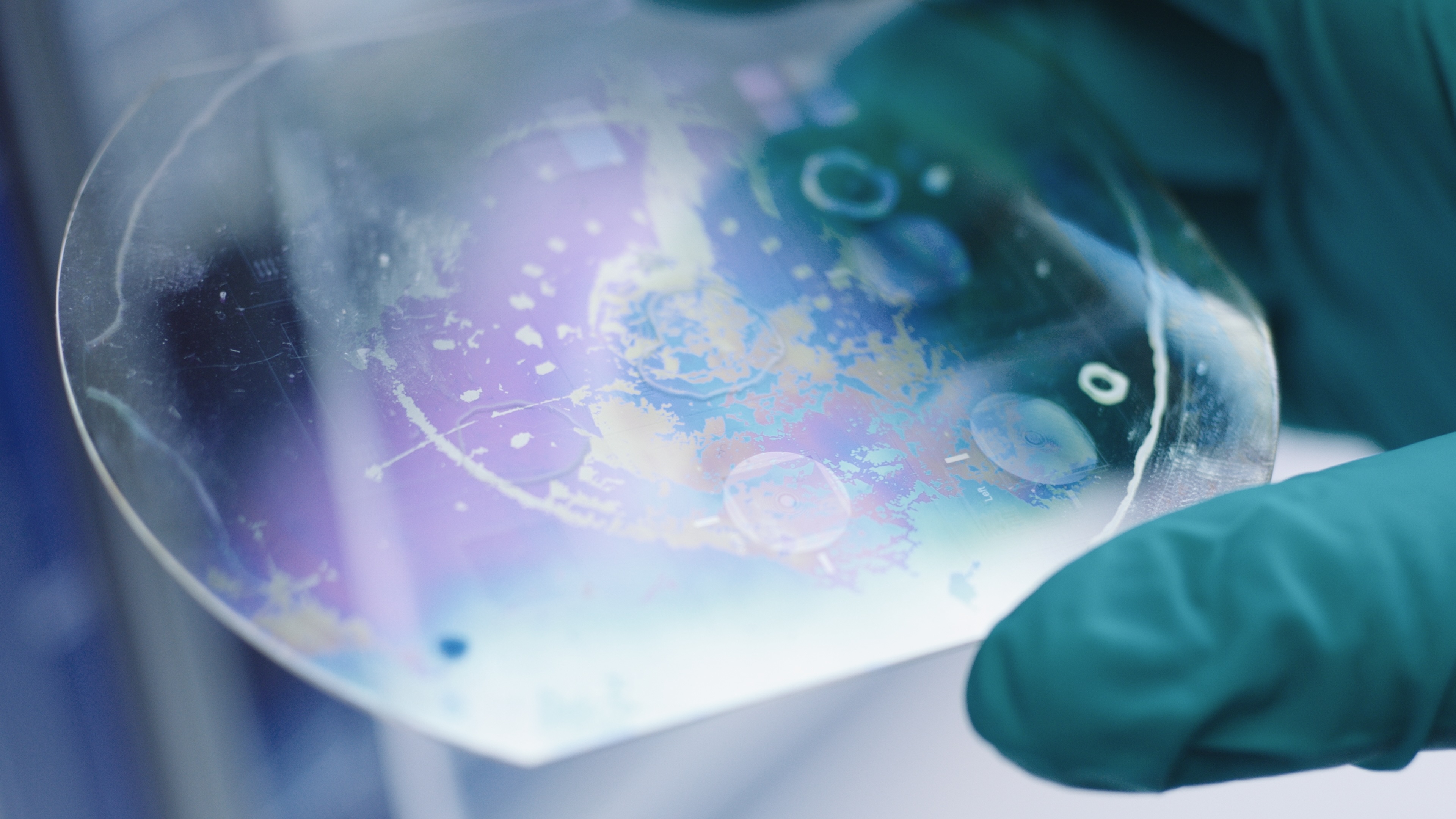
Figure 1: The Z1 is an ideal tool for rapid, automated assessment of optical surfaces, such as those produced via nano-imprint lithography or other classical lithographic processes.
Nano-imprint lithography (NIL) is a powerful and cost-effective tool for fabricating complex optical structures down to the sub-micrometer scale. Reliable device performance, however, means ensuring that these features ultimately match their intended design - even small deviations (i.e. tens of nanometers) to their dimensions, shape fidelity, and refractivity can critically affect optical behavior.
The challenge of characterizing NIL-based optical devices is that we require both high spatial resolution and coverage over millimeter-scale fields of view – something conventional topology-scanning methods, such as SEM, AFM, ellipsometry and white-light interferometry cannot provide efficiently. As a result, characterizing NIL-based optical devices means compromising between the following:
- Throughput: SEM and AFM are too slow for quality control over large areas.
- Geometry limits: AFM probes cannot accurately capture high-aspect-ratio features, leading to underestimated depths.
- Surface restriction: SEM and white-light interferometry reveal only surface morphology, not refractive or subsurface variations.
- Sample alteration: Conductive coatings used in SEM obscure surface geometry and prevent direct dimensional comparison to design data.
A new approach with the ClairSci Z1
We show how Quantitative phase imaging (QPI) overcomes these limitations by measuring both the attenuation and optical phase delay of white light transmitted light through transparent or semi-transparent NIL structures. The resulting maps of local thickness and refractive index then provide a complete, non-destructive assessment of both geometry and optical performance - in seconds. This enables:
- 3D structural mapping across entire device areas
- Quantitative comparison between measured and designed feature dimensions
- Detection of spatial variations in refractive index and uniformity
- Automated, high-throughput analysis with remote monitoring
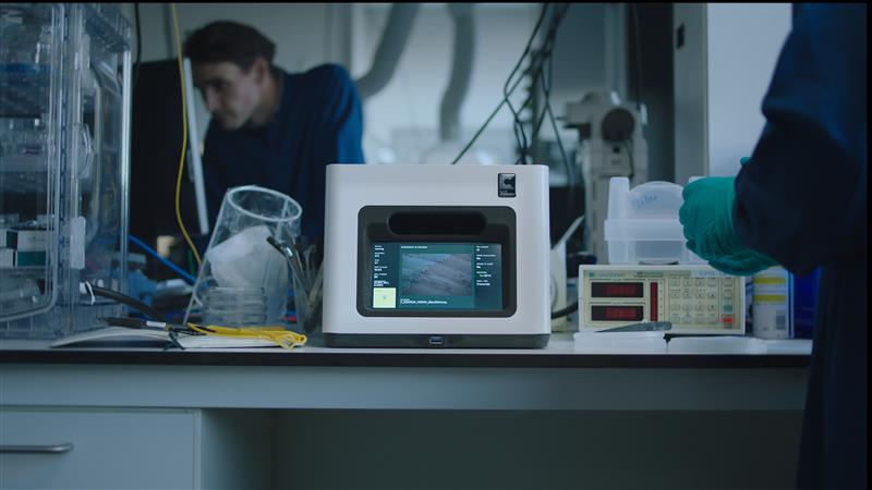
Figure 2: The Z1 is a compact and cost-efficient way to add quantitative optical characterization to any laboratory or production area, and is built to withstand the requirements of these environments
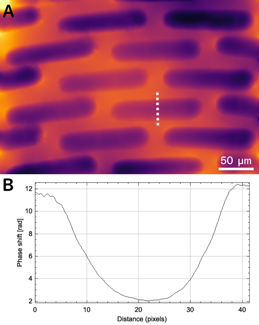
Sample and measurement details: The NIL optical device consisted of a lattice of cross-shaped features on a transparent polymer substrate. The sample was mounted between two No. 1.5 coverslips (170 µm) using immersion oil (n = 1.515) to minimize refractive mismatch.
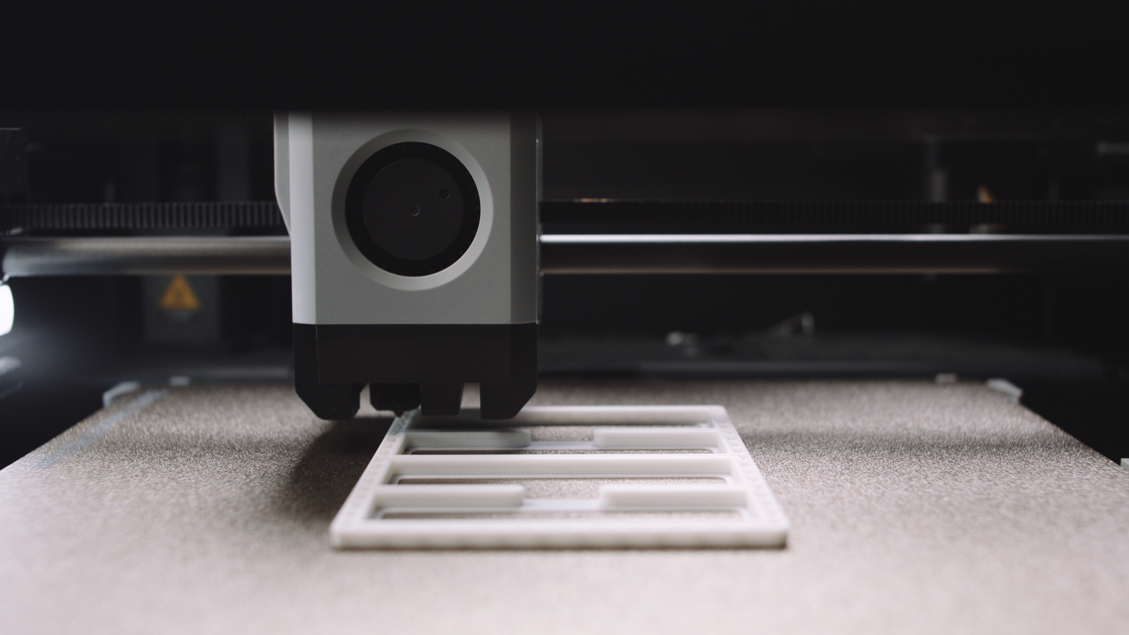
Figure 3: Custom-designed sample holders were 3D printed based on models provided on the Clair Scientific website. These enable ideal mounting and imaging conditions for every sample and experiment type
Measurements were then performed on a ClairSci Z1 equipped with a 40× Nikon Plan Fluor objective (NA 0.7). Automated calibrations and flat-field correction were performed prior to imaging. Illumination intensity was set to 80 % with a 30 ms exposure time, providing high signal-to-noise ratio with minimal motion artifacts. Each 1 mm × 1 mm field of view was acquired in ~4 seconds as so to allow for comprehensive scans of large device areas.
Results & Discussion
3D mapping: Phase-derived thickness maps revealed detailed 3D profiles of the NIL lattice with sub-micron precision. Central regions exhibited variable feature heights from the center of the structure to the peripheral regions, potentially indicating non-uniform imprint pressure.
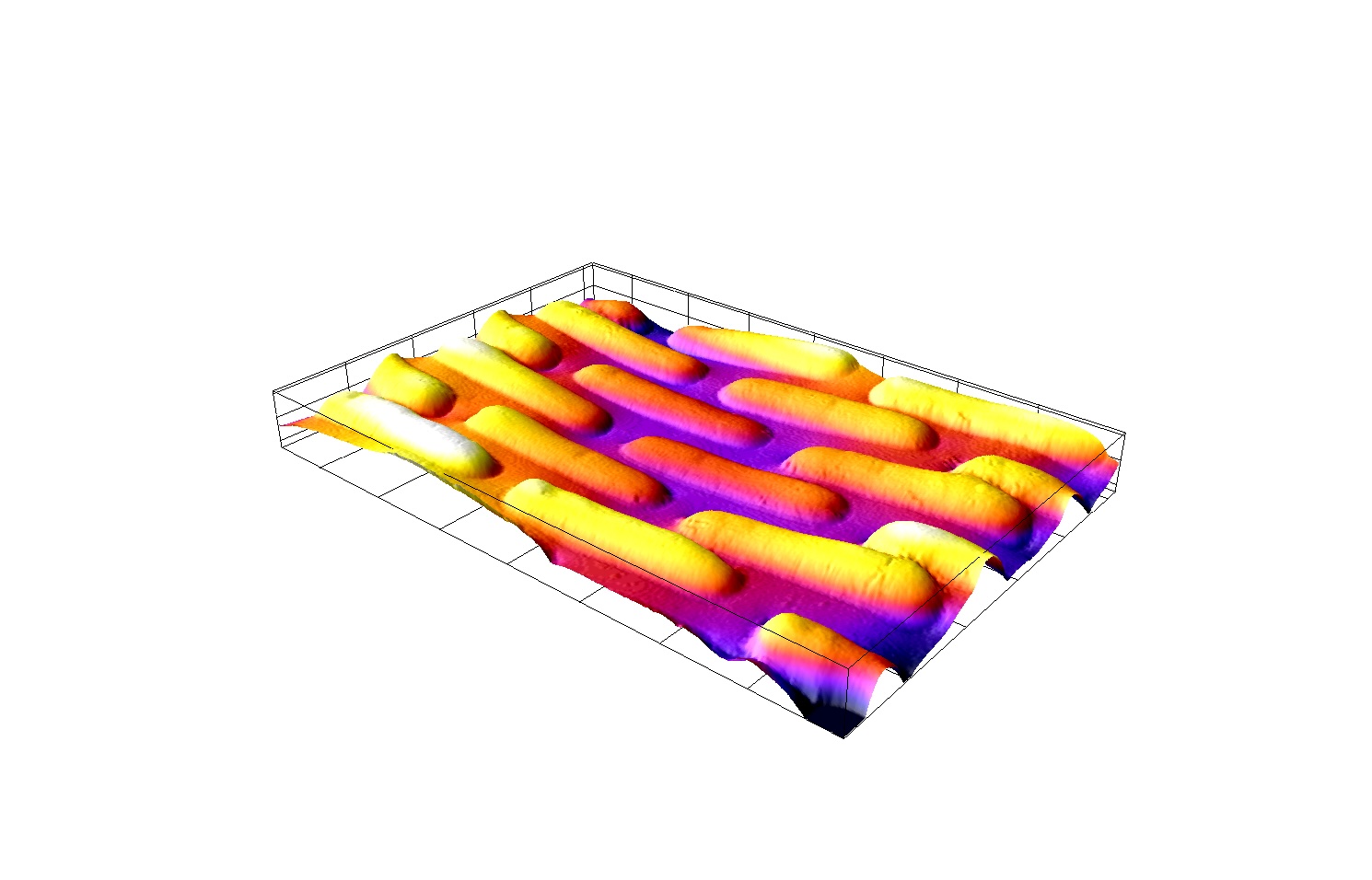
Optical performance: At 632 nm, the reconstructed phase map showed phase variations across the structures of ~10π, in close agreement with the intended design values at this wavelength. This correspondence between dimensional and phase data confirms the ability to directly relate geometric non-uniformities to optical performance deviations.
The Z1’s rapid, quantitative imaging enables immediate feedback during NIL process optimization. Systematic variations - such as reduced imprint depth near device edges - can be identified and corrected by adjusting pressure or substrate temperature. The short acquisition time (~4 s per field-of-view) supports statistical mapping of multiple devices or process batches, facilitating high-throughput quality control.
Moreover, the combination of thickness and refractive-index information provides direct input for optical modeling, allowing predicted device behavior to be validated against experimental data before final integration.
Conclusions
Quantitative phase imaging with the ClairSci Z1 offers a fast, non-destructive, and fully automated solution for characterizing nano-imprinted optical devices. The ability to extract both structural and optical parameters from a single dataset eliminates the need for separate metrology techniques and accelerates iterative design cycles. Crucially, this approach enables reliable verification of NIL device quality, and lays the foundation for more efficient development of advanced photonic components.